
 English


Which is the future ? 182mm cell VS 210mm cell
By the end of 2020, China's silicon wafer output is 134.6GW, up 25.7% year on year, accounting for 98% of the global output.
The dependence of the whole photovoltaic industry on China's production capacity is becoming more and more obvious.
At the same time, the competition of domestic silicon wafer manufacturers has not stopped for a moment. Nowadays,
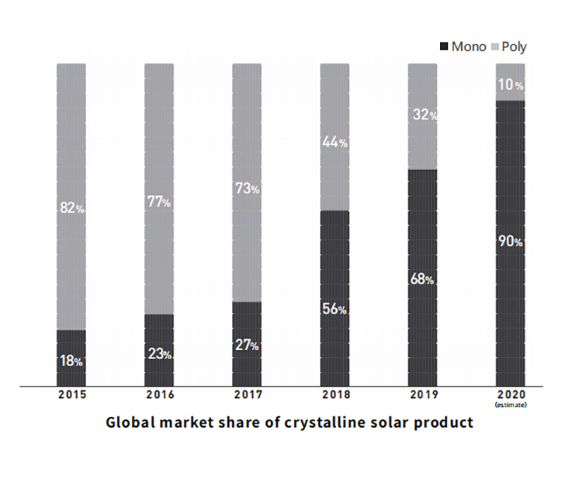
monocrystalline silicon dominates the market in monocrystalline silicon and polycrystalline silicon, while the market has not
given an accurate answer in the size of silicon wafer.
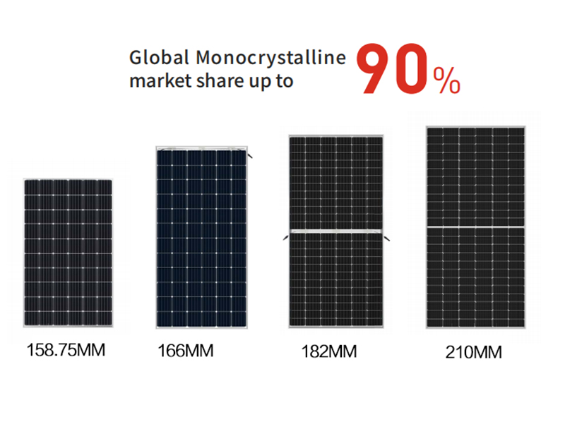
The debate over the size of silicon wafers began as early as five years ago. In 2015, Longi and Zhonghuan jointly customized the M2
size standard, which is also the current mainstream size. The side length is 156.75mm, the diagonal length is 210mm, the area of
each silicon wafer is 24432mm, and the market share is about 80%.
Since 2018, various players have released silicon wafers of different sizes, such as 157mm, 158.75mm, 161mm, 163mm, 166mm,
180 + mm and 210mm.
Since then, Longi's M6 size new products have been launched, triggering the SNEC exhibition that year. Its side length is 166mm,
diagonal diameter is 223, and silicon area is 27412 square mm, which is 12.20% larger than M2 size. 166 silicon chip fully takes
into account the compatibility of the old production capacity of silicon chip, battery and module before 2019, and the cost of silicon
chip, battery and module transformation is the lowest. It can be said that 166 is the best silicon chip size for the old production
capacity, and it is the easiest to promote a large number of products, which can be proved by the substantial increase of market share.
On August 16, 2019, Zhonghuan applied semiconductor technology to the photovoltaic industry. The first large-size silicon chip with
a side length of 210mm was launched. The silicon chip area reached 44092mm, 80.47% larger than the current conventional product
m2, leading the photovoltaic industry into a new stage of large-size.
Large size silicon wafer is the best choice for the industry to reduce cost and increase efficiency. However, due to the different sizes of
silicon wafers used by enterprises, the manufacturing costs of photovoltaic industry chain, including silicon wafers, batteries, modules
and glass, have risen sharply.
Therefore, people in the industry object to the 210 large-size silicon wafer launched by Zhonghuan, because there are problems in hot
spot, chip loss, split, bracket and inverter compatibility in the current 210 production. The objectors think that this is completely
abandoning the constraints of existing production capacity on the idea and selecting the optimal silicon wafer size based on the
assumption that the cost of new production capacity is optimal.
Using larger silicon chips to further reduce the cost, the 182mm and 210mm routes not only aroused the discussion of the industry,
but also became the focus of public attention. The two camps of 182mm and 210mm silicon wafers expressed their own views on
technology and development.
The 182 silicon chip camp is mainly represented by Longi, Jinko, JA, Artes, Jiangsu Runyang Yueda, Jiangsu Zhongyu photovoltaic
and Lu'an solar. They jointly advocate the establishment of the 182mm * 182mm photovoltaic silicon chip standard (M10), which
will be 182mm * 182mm × 182mm wafer size is the standard size for developing the next generation of wafer, battery and module
products. The purpose is to avoid the rise of manufacturing costs of auxiliary materials in the photovoltaic industry chain, including
silicon wafers, batteries, modules and glass, due to the different sizes of silicon wafers adopted by various enterprises, promote the
establishment of a unified standard based supply chain system in the whole industry, realize the standardization of equipment
manufacturing system and customer application system, and promote the healthy development of the whole industry.
To a certain extent, 182 silicon chip takes care of the compatible ability of silicon chip, battery and module production line, and the
ability to reduce cost and increase efficiency is better than 166 silicon chip. For component enterprises, compared with 210mm,
182mm silicon wafers and size cells are easier to buy in the market.
The 210 silicon chip is represented by Zhonghuan. The 210 silicon chip has the strongest ability to reduce cost and increase efficiency.
It is fully compatible with the future photovoltaic technology. Whether it is n-type battery technology or the superposition with perovskite,
the 210 will be the standard in the future. In addition, the pressure of affordable access to the Internet will significantly enlarge the
difference between the two, forcing customers to choose the products with the lowest electricity cost.
It can be said that the two are striving for the present and focusing on the future. There is no difference between good and bad.
Conforming to the historical trend will eventually be absorbed by the times. And often the present is the foundation of the future,
and the future is the continuation of the present. Social progress is bound to be accompanied by the replacement of technology.
Survival of the fittest is the inevitable result of social development. Which technology should be extended? We should not only look
at the existing conditions, but also focus on the future development.
From the current form, 180 + wafers suitable for the production conditions of all links of the current industrial chain are more easily
accepted by the market, and the initial coverage will be wider than that of 210 wafers. With the progress of technology, the existing
210 silicon technology bottleneck has been broken, and the scale of production has been expanded. At that time, the market will
give a new answer.
Categories
latest blog

To be leader of global manufacturer of high-performance PV products.
For inquiries about our products or pricelist, please leave to us and we will be in touch within 24 hours.
© Copyright: 2026 Sunetraco All Rights Reserved.

IPv6 network supported

